Researchers work out how to control 2D semiconductor growth for future chips
News Source : Theregister.com
News Summary
- Korean boffins use oxygen to stop crystals forming in the wrong places, aiming to get tech to commercial sector by 2030.
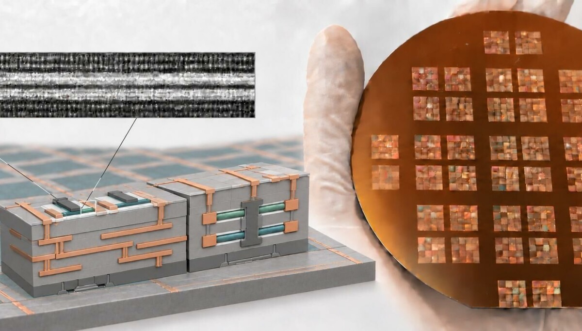
- The technique uses an etching flux to suppress the formation of new crystals everywhere within each patterned growth region except at its geometric center.
- When grown on a wafer, however, 2D semiconductor crystals typically start forming at random points, or "nucleation events occur stochastically at random sites within the growth region," as the paper puts it.




















 Never miss a story from us, subscribe to our newsletter